Introduce of printed circuit board film

Film making is the previous printed circuit board or flexible pcb manufacturing process, the quality of film directly affects the quality of PCB product. In the production of a certain kind of PCB, it must have at least a corresponding film negatives. Each printed conductive pattern (circuit layer, the signal layer, the power level layer) and non-conductive pattern (solder mask and silkscree) should have at least one film negatives. By photochemical transfer of technology, the patternswill be transferred to the production pcb board.

Film negatives application in the PCB production for the following:

1. Photographic mask pattern transfer in the graphic, including circuits graphics and solder line graphics.
2. Screen Printing in the production of screen templates, including soldermask and silkscreen.
3. For Machining (drilling and milling appearance) based programming CNC machine tools and drilling information.

With the development of the electronics industry, the increasing higher of requirements of PCB. PCB design of high density, thin wire, small diameter tend to become increasingly fast, PCB production processes become more perfect. In this case, if no high-quality film negatives, can produce high quality printed circuit boards.In this case, if no high-quality film negatives, we can’t produce high quality printed circuit boards.
PCB development trends of advanced manufacturing technology

Summary of domestic and international manufacturing technology for the future development trends of PCB production is basically the same discourse: namely high-density, high precision, small hole diameter, fine wire, fine pitch, high reliability,multi-layered, high-speed transmission, lightweight, thin thickness development, and in production to improve productivity, reduce costs, reduce pollution and meet the many varieties and small batch production direction.
As printed circuit boards level of technological development, we often use the line width, diameter, thickness / diameter ratio as the representative. Please see the level of PCB development process as follows:

Level of development of printed circuit boards technology:

Years
 1970
 1975
 1980
 1985
 1990
 1995
 2000

Aperture (mm)
 1.0
 0.8
 0.6
 0.4
 0.3
 0.15

Width (mm)
 0.25
 0.17
 0.13
 0.10.
 0.08
 0.05

Thickness / aperture ratio
 1.5
 2.5
 5
 10
 20
 40

 Hole density, number of holes / CM2
 4
 7.5
 15
 25
 40
 55

CMD Circuits is engaging in manufacturing the high quality and competitive cost printed circuit boards and flexible pcb for our customers.

Outline processing of flexible cirxuits

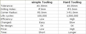
Outline processing of flexible circuits usually use punching method. The tooling we have two kinds: simple tooling and hard tooling for punching.  Please see below the differences between these two molds:

Stripping of Flexible circuits

Stripping of flexible circuits is intended to clear resist layer to expose the copper on the board after etching. Does operation of stripping of flexible circuits going smoothly, dependent on equipment design and preparation of the liquid two main parts.

Stripping is relative simple compare to etching of flex circuit with the complex machine. But the “film residue” filtering, and recycling waste shall be disposed properly.

The chemical liquid of stripping, generally use the traditional NaOH(based),solution concentration is about 1-3% in weight, and temperature of the solution between about 40-55 ℃. The major reasons to use the NaOH in our industry: for dry film with good solubility, low prices and easy got. However, according to the actual use of that low concentration of NaoH work not very well, so now the mostly use KoH instead of NaoH as the solution for stripping.
The chemical properties of KoH and NaoH are very similar, but because of the dissolution of K for the dry film with excellent performance, and enhance the effect of stripping. This way don’t need to change the existing production equipments and the filtering effect of the film residue are improved.

The problems appear in etching process

Do you know what problems will appear in etching process of flexible circuits? Ok, follow me to know the details:

1) Etching speed is geeting slower
This is usually because of the low temperature, low spray pressure or chemical proportion of etching solution. But if  these conditions under well control, the etching speed slow may be due to the dissolution copper content is too high. At this point, it is necessary to adjust the etching solution.
2) Precipitation appear in solution
This is due to lack of complexing agent Cl-, or the dilution caused by water. Precipitate is Cu2Cl2: insoluble in water.
3) Resist layer is damaged:
When excess acid is being, this phenomenon appeared. Especially in higher temperatures will appear. Now we can replaced by NaOH or water to adjust. If the acid concentration and the conditions are suitable, then the problem may be due to  improper cleaning of the board or exposure of flexible pcb.
4) The yellow residue in the copper surface
This residue is generally copper hydroxide, which does not dissolve in water. When the board is etched or alkaline cleaning to as the residue left on the board. In addition, when Cl-concentration and the acidity is too low in etching solution, after etched the white precipitate appeared on board, which may be insoluble Cu2Cl2 precipitation. Now we can use 5% hydrochloric acid solution to wash, and last wash by water.

When we know the above problems will appear in the etching process of flex circuits, so we will make the well quality controlling system to control these problems, and then ensure high quality flexible circuits, flex pcb.

Flexible circuits Developing Quality Check

Let’s tell you one way to check the trace quality is good or not after developing of flexible circuits. After developing, even if some developing trace is dirty, or the base is long, is unable to check them out with a magnifying glass; but Cucl2 test is a non-destructive testing way. Testing methods are as follows:
1) First to clean the flexible pcb surface after developing, for example:
After developing → acid washing → acid etching → acid 
2) in a 5% Cucl2 solution for 30 seconds, the best to swing liquid slightly, and use a sponge to remove small air bubbles on the board to invoid to affect judgments.
3) washed
4) drying
5) visual inspection
The copper surface of normal developing will form a layer of gray and black oxide layer after handling.  When the  surface of flex pcb with dry film glue, there will still maintain a bright copper color. This method can be tested if developing of flexible circuits is good.

Related Posts:
1.Drilling of flexible circuits;
2.FPC Exposed Process Operation Notes.

Solution configuration of FPC developing process

Developing process of flexible circuits is the unexposed active group of photographic film part response to dilute alkali solution to the produce soluble substances and dissolve, leaving the already sensitive graphical circuit pattern. The most common used liquid is made of Na2CO3, weight content ratio between 0.75% and 2%.

Dry or wet film load is small, so the correct solution configuration of flexible pcb is the most basic step, in order to accurately control the concentration, we use acid-base titration method calculate the concentration of Na2CO3.
Reference to below methods:
(1) Sampling 25ml developing liquid in 250ml beaker;
(2) by adding D.I. water 100ml and 3-5 drops of methyl orange;
(3) use 0.1N hydrochloric acid to titrate the color changed to red;
(4) Calculate: wt% Na2CO3 = 0.0212 × titre (ml).

Usually dry film in 1% Na2CO3 developing liquid, the loading is about 12-15 mil-ft2/gal. At a higher developing pressure and under the full water washing can be obtained higher loading.

DI water, soft water is recommended for developing of flexible circuits, the use of hard water would have caused the hard dirt to clog of the nozzles.

FPC Exposed Process Operation Notes

Today follow me to know the FPC exposed process operation notes, exposed is the very important step of making flexible circuits.

(1) The vacuum framework of exposure machine is essential, vacuum degree≥ 90%, only through the vacuum machine to let film tightly with the base substrate, and to ensure that no distortion of the circuits in order to improve accuracy.
(2) After the exposed, should immediately remove the panels, otherwise peripheral vision of light will cause unwanted film in developing of flex circuits.
(3) Working conditions must be met: clean (10,000 scale or higher) operating under yellow light, indoor temperature and humidity (21 ± 1 ℃, 55 ± 5%). Exposed machine should have the cooling air exhaust system.
(4) Exposed, the film emulsion side must face down, and  firmly stick the light-sensitive surface side to improve the resolution for circuits.
(5) Exposed machine should regularly calibrate to ensure accurate exposure.

Related Posts:
1. The structure of FPC;
2. Flexible Circuits Production Process;
3. The stiffener of flexible circuits.

FPC Enhance Board

FPC enhance board is the stiffener glued to the local position of flexible circuits. It can support the substrate of flexible, and convient to flexible PCB  connection, fixed, plug components or other functions. FPC enhanced board material to be choose according to different purposes.

Often flexible PCB need to bending and do not want too much mechanical strength and hardness, but the components or connectors assembly location need the appropriate material for the FPC enhanced board.

Methods of saving PCB cost

In order to let the cost of PCB can be as low as possible, there are many factors that must be taken into account:

1. The size of the board is most important. The smaller board, the lower the cost. Part of the PCB has become the standard size, as long as the cost according to size as it will naturally decrease.
2. SMT will be much lower than THT, because the components on the PCB will be more intensive (also small).
3. On the other hand, if the components on the board is very dense, then the routing must also be more detailed, and the equipments should be correspondingly higher required. The cost of these problems,compare to reduce the PCB size with more savings.
4. The more layers the higher the cost.
5. Drilling takes time, so NTHs the less the better.
6. Buried holes is more expensive than NTHs. Because the buried hole must be drilled at the junction.
7. Hole size.
8. Others.

Last, the equipments in manufacturing is more complicated, the cost will be more high. Understanding of PCB manufacturing process is very useful to save the cost. CMD Circuis have professional working group to analyze and control the cost of material.

Pages: Prev 1 2 3 4 5 6 7 Next